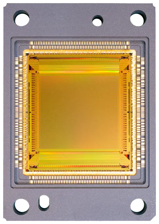
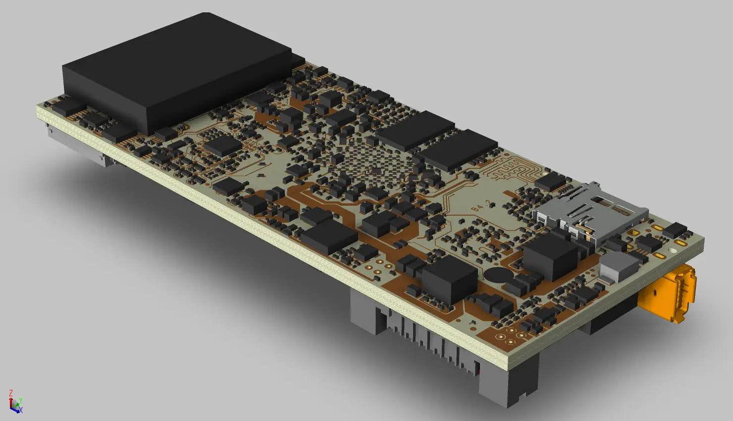
Our lock-in image sensors and camera boards are the key components for developing your own sensor products. They offer OEMs a proven technology platform that enables maximum precision, reduces development risks, and significantly shortens time-to-market.
The development of CMOS image sensors and FPGA-based high-performance cameras, along with our many years of experience in optical metrology, form the basis of our components: lock-in image sensors, camera boards, firmware/signal processing, and matched optics. Documented interfaces (including GenICam), SDKs, and reference designs enable rapid integration into your OEM sensor products.
Patented heliSens™ in-pixel signal processing: parallel demodulation in the array, internal sample/demodulation rates up to 1 Mfps. For modulated measurement principles with high SNR and ambient light suppression; external frame rates up to 5 kfps.
FPGA-based further processing for shortest latencies – optimally matched to heliSens™ image sensors. Versatile I/O interfaces, trigger & synchronization for tight control integration; GenICam enables simple, robust integration into your image processing software.
Lock-in algorithms with I/Q averaging, phase/amplitude extraction, and surface extraction. Streaming pipelines with deterministic timing. Documented APIs/SDKs (C/C++, C#, LabVIEW) and example code accelerate integration.
Matched optics, filters, and mounts for reproducible signals – complemented by calibration targets, cable sets, and mechanics. If required, validated for temperature/EMC and released for series production.
Our experience and technologies are available to OEM customers for their own sensor products. If required, we support you in development (sensor IP, FPGA/embedded, optics), undertake adaptations, and parts of manufacturing and logistics – also as custom development. Exclusively for OEM series.
Decades of experience in CMOS sensor design, from pixel architecture, lock-in pipelines, and parallelized in-pixel processing to readout/timing design. The basis for OEM projects is the patented heliSens™ technology and adaptable CMOS sensor IP.
Development of camera and processing boards with FPGA pipelines for deterministic latencies. Design of high-speed I/O, trigger/synchronization, and clock distribution; signal/power integrity, thermal/EMC design, and DFM/DFT up to series release.
We efficiently implement customer-specific requirements with a modular software stack: micro-code directly on the image sensor, FPGA firmware for parallelized algorithms, and embedded Linux for smart camera applications. Adaptations and co-development are possible for OEM projects.
If required, we take over partial manufacturing and the supply chain of core components: selection/qualification of manufacturers, procurement and bill of material management, test/EOL tests, and continuous traceability. Forecast and framework contract-based scheduling, second-source/obsolescence management, and defined quality and delivery plans ensure series supply.